
Overview
Circuit boards need fine, permanent, traceable marks that survive assembly and won’t contaminate the board. UV and CO2 both do it cleanly, with no contact and no ink.
Why UV (and CO2) Work on PCB
UV at 355 nm marks cold and ultra-fine — down to 0.01 mm line width — so it places clear 2D codes and serials on dense boards without heat stress, the right choice for FPC and high-density PCB. CO2 at 10.6 µm suits marking solder mask and board surfaces where detail is less critical.
Built to Last
The mark is a change in the surface itself, not ink, so it survives reflow, cleaning and handling — and reads reliably as a 2D code through the product’s life.
Specs That Matter
UV 355 nm (cold, ultra-fine 0.01 mm line width) for dense boards and FPC; CO2 10.6 µm for surface marks. Fields 100–300 mm, matched to the board.
How to Mark a PCB
- Fixture the board and set the focus to the surface.
- Import the code (serial, 2D, logo) and set UV parameters.
- Run a sample, check code readability and that the board is unstressed, then save the recipe.
- Set repeat positioning and start the batch.
- Scan the codes and log first-article approval.
Applications
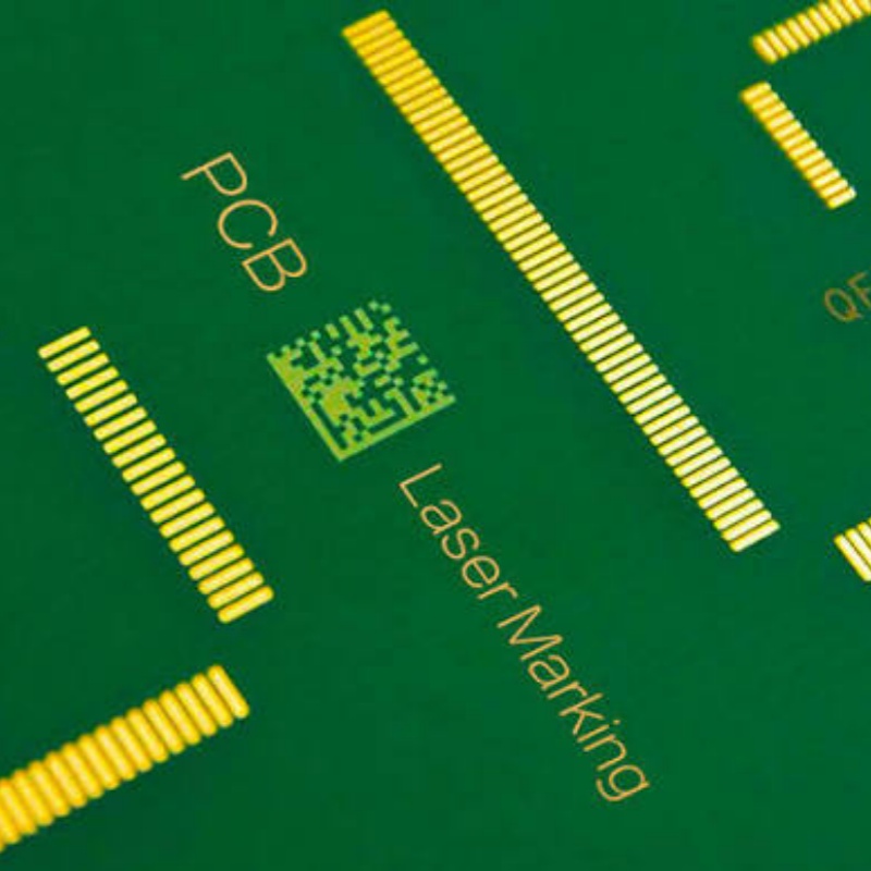
Traceability and 2D codes on PCB and FPC, solder-mask marking, component and connector marking, electronics housings.
CE Compliance
CE-marked, with conformity documentation available on request. We never claim SASO, SABER, GCC or UKCA we do not hold.
Getting It Right Before You Buy
Send us a board. We’ll mark it on UV, check code readability, then quote against it.
Request a Quote · Download the Spec Sheet
Explore: Non-Metal Marking. Related: UV Marking · QR & Code Marking.